- 您现在的位置:买卖IC网 > Sheet目录220 > DLP3V3DTZ-7 (Diodes Inc)TVS DUAL-UNI SGL-BI 372W SOT23-3
NOT RECOMMENDED FOR NEW DESIGNS
DLP3V3DTZ
DUAL UNIDIRECTIONAL AND SINGLE BIDIRECTIONAL TVS
General Descriptions
?
This Transient Voltage Suppressor (TVS) diode is designed for
dual unidirectional or single bidirectional protection for data
lines, components or circuits from damage due to electrostatic
discharge (ESD), cable discharge events(CDE) and lightning
(see IPPM below). It offers high ESD capability, low reverse
leakage, low junction capacitance and low clamping voltage
over range of temperature. They are suitable for computers,
communication systems, hand held portables, high density PC
boards and peripherals.
Features
?
?
372 Watts Peak Pulse Power (tp=8/20 μ S)
AEC-Q101 (Human Body Model- 8kV, Machine Model-400V)
GND
3
N/C
3
and 25 kV(air)/ 8 kV(contact) as per IEC61000-4-2(ESD)
?
?
?
?
Dual Unidirectional and Single Bidirectional Configuration
Lead Free By Design/ROHS Compliant (Note 2)
"Green" Device (Note 3 & 4)
Surface Mount Package Suited for Automated Assembly
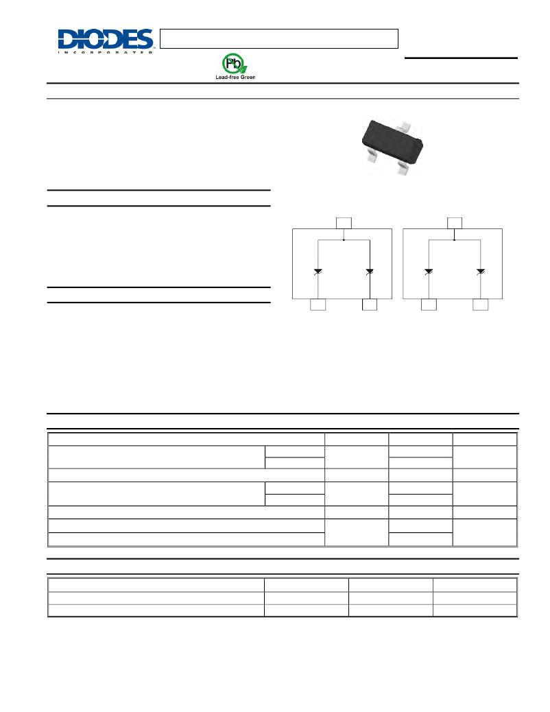
D1
D2
D1
D2
Mechanical Data
?
?
Case: SOT-23
Case Material: "Green” Molding Compound (Molded
1
Line1_in
2
Line2_in
1
Line_in
2
GND
?
?
Plastic). UL Flammability Classification Rating 94V-0
Moisture Sensitivity: Level 1 per J-STD-020
Terminal Connections: See Fig. 1
A. Unidirectional Protection
for two Lines
B. Bidirectional Protection
for a single Line
?
?
?
?
Terminals: Finish - Matte Tin annealed over Alloy 42
leadframe. Solderable per MIL-STD-202, Method 208
Marking & Type Code Information: See Page 6
Ordering Information: See Page 6
Weight: 0.008 grams (approximate)
Fig. 1: Schematic and Pin Configuration
Absolute Maximum Ratings
@T A = 25°C unless otherwise specified
Characteristic
Symbol
Value
Unit
Peak Pulse Power (tp=8/20 μ S)
Continuous Power Dissipation (Note1)
Maximum Peak Pulse Current (tp=8/20 μ S)
Forward Surge Current (8.3 ms half sine-wave)
ESD per IEC 6100--4-2(air)
ESD per IEC 6100--4-2(contact)
Unidirectional
Bidirectional
Unidirectional
Bidirectional
P pp
P D
I PP
I FSM
V pp
372
145
300
40
15
10.5
± 25
± 8
W
mW
A
A
kV
Thermal Characteristics
C
Characteristic
Operating and Storage Junction Temperature Range
Thermal Resistance, Junction to Ambient Air (Note1)
Symbol
T j , T stg
R θ JA
Value
-55 to +150
420
Unit
°
°C/W
Notes:
1. Device mounted on FR-4 PCB, 1 inch x 0.85 inch x 0.062 inch; as per Diodes Inc. suggested pad layout document AP02001 on our website
2. No purposefully added lead.
3. Diodes Inc.'s "Green" policy can be found on our website at http://www.diodes.com/products/lead_free/index.php.
4. Product manufactured with Date Code 0627 (week 27, 2006) and newer are built with Green Molding Compound. Product manufactured prior to Date
Code 0627 are built with Non-Green Molding Compound and may contain Halogens or Sb2O3 Fire Retardants.
DS30669 Rev. 3 - 3
1 of 8
DLP3V3DTZ
? Diodes Incorporated
发布紧急采购,3分钟左右您将得到回复。
相关PDF资料
DLPA004-7
DIODE SW 85V 200MW SOT-363
DLPA006-7
DIODE SW 85V 200MW SOT-363
DLPD3V3LC-7
TVS BIDIR 330W 3.3V SOT-26
DLPT05-7
TVS 6V 300W SOT23-3
DM-31-1
DPM LED 2V 3.5DIG RED SGL BOARD
DM-3100B-1
DPM LED 2V 3.5DIG AC-POWERED RED
DM-3100N-1
DPM LED 2V 3.5DIG LO PROFILE RED
DM-4101L-1
DPM LED 2VDC 4.5DIGIT RED
相关代理商/技术参数
DLP-408-R2
制造商:ITT Interconnect Solutions 功能描述:
DLP4500
制造商:TI 制造商全称:Texas Instruments 功能描述:DLP 0.45 WXGA DMD
DLP4500FQD
功能描述:显示驱动器和控制器 DLP 0.45 WXGA DMD
RoHS:否 制造商:Panasonic Electronic Components 工作电源电压:2.7 V to 5.5 V 最大工作温度: 安装风格:SMD/SMT 封装 / 箱体:QFN-44 封装:Reel
DLP4500FQE
功能描述:显示驱动器和控制器 DLP 0.45 WXGA DMD
RoHS:否 制造商:Panasonic Electronic Components 工作电源电压:2.7 V to 5.5 V 最大工作温度: 安装风格:SMD/SMT 封装 / 箱体:QFN-44 封装:Reel
DLP4500NIRFQE
功能描述:IC WXGA DMD .45 80LCCC 制造商:texas instruments 系列:* 零件状态:有效 标准包装:5
DLP4501FQG
功能描述:IC WXGA DMD .45 制造商:texas instruments 系列:* 零件状态:有效 标准包装:70
DLP4710FQL
功能描述:IC CTRLR DGTL DLP4710 100CLGA 制造商:texas instruments 系列:* 零件状态:有效 标准包装:1
DLP5500
制造商:TI 制造商全称:Texas Instruments 功能描述:DLP? 0.55 XGA Series 450 DMD
